TSMC 2nm: When in Production & A14 Node Development?
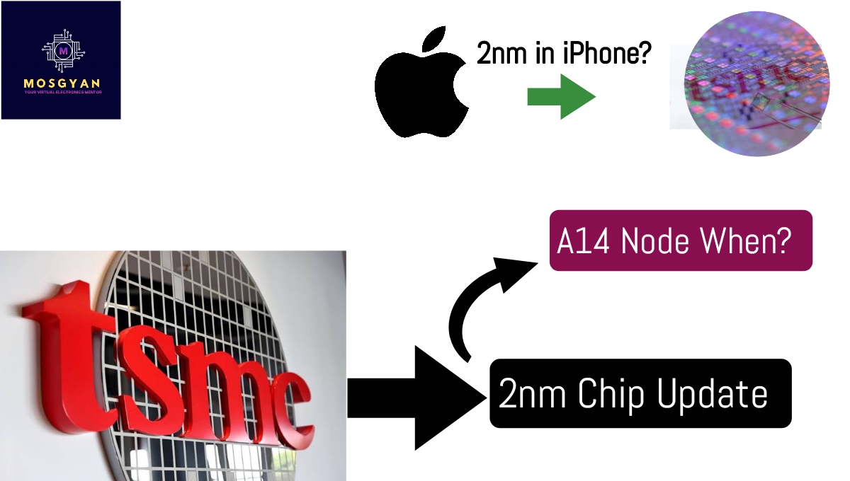
Taiwan semiconductor manufacturing semiconductor (TSMC) is world’s biggest foundry. They cater the biggest companies across globe reason being superior performance of their advanced node in terms of power, yield & efficiency. TSMC 2nm is the latest tech node which is supposed to get into the mass production by the 2nd half of 2025. This 2nm process of TSMC supports GAA (Gate all around). There are further few more variants of N2 is supposed to arrive starting from N2P & then N2X.
Since N2 is planned for 2nd half of 2025 due to that N2P production will start in late 2026. N2P is the enhanced power variant of N2 & N2X is the voltage enhanced variant of N2. TSMC hopes that N2 will improve performance by 10%, Reduce power by 20% & increase chip density by 15% compared to their N3E Tech node. Earlier TSMC announced in the technology symposium that their 2nm tech node will be able to support backside power delivery which is not supported in the N2P chips as it will continue to use regular power delivery circuit.
Nanoflex feature addition in TSMC 2nm chips:
TSMC’s 2nm chip family will add nanoflex capability in its chips. This feature helps designers to mix various cells from different libraries. This is a great addition as designers can mix different cells such as area efficient or high performance or low power cells from different libraries & can make a best PPA suited chipset. Similar feature was also given in TSMC’s 3nm process & it is called as FinFlex there.
TSMC 2nm Wafer Prices:
TSMC has hiked the silicon wafer prices for 2nm process. For N3 (3nm) process TSMC was reportedly charging $20,000 for wafer. Whereas if reports are assumed to be than TSMC has hiked the silicon wafer price around $30,000 for its 2nm process which is equal to 50% hike compared to N3 tech node. However this price hike is mainly due to the complex manufacturing challenges associated with this tech node. TSMC 2nm process will use GAA FET where Gate will be in contact with channel on all sides.
Is Apple going to use TSMC 2nm chips in iPhone 17 series?
Apple is the primary customer of TSMC & they have been using the latest tech node of TSMC in their iPhone series. So, it was believed that iPhone 17 series will be the first set of smartphones which will use TSMC 2nm chips. However as per some reports iPhone 17 is supposed to use TSMC’s 3nm (N3P) tech node whereas TSMC 2nm chips can be seen in the iPhone 18 series.
One of the reason behind this claim is that 2nm process mass production is schedule to take place by the end of 2025 & before that apple will reveal its iphone 17 series but there are few reports which also indicates that TSMC is accelerating the production process so that stable yield can be secured for mass production. We will have to wait for some more time to get some official confirmation on this.
In this 2nm race TSMC is not the only foundry, there are various other giants as well along with some new comer entries. Intel & Samsung are also expected to ramp up their 2nm development. In the new foundries there is one Japanese foundry named as “Rapidus” which is working on 2nm chip production. However the timeline of Rapidus 2nm production is quite late compare to TSMC 2nm but it’s a great initiative from this Japanese foundry as they are building foundry from scratch to revive Japan’s semiconductor hopes.
In case if you want to know more about Rapidus’s 2nm chip fabrication plan, please read this article of Mosgyan:
Rapidus 2nm Chip Production: A Threat for TSMC?
TSMC’S 1.4nm Update:
What’s next after TSMC 2nm? Well to answer that TSMC has already started development of 1.4nm. It will officially be called as A14 tech node. Although it is not officially confirmed yet that when will TSMC start the mass production for A14 but as the timeline for N2 is scheduled for 2025 end & for N2P it is by the 2nd half of 2026 so it is safe to assume that A14 will only come into production after 2026. Maybe in 2027 or in the beginning of 2028.
There are lot of questions related to A14 tech node like will A14 use vertically stacked Complementary FET or not? Which kind of litho machines will be used for A14? There are so many questions like this whose answer is expected in near future.


