CMOS Inverter: Basic Theory & design Challenges in lower tech nodes
CMOS inverter is the basic building block of any digital circuit. Through appearance it looks very easy circuit to understand a PMOS & a NMOS, that’s it. Even during under-graduation many of us skip this part assuming its very easy and any kind of question asked in exam can be answered easily. This is partial truth. CMOS Inverter topic is easy to navigate but there can be various kind of questions can be formed using this topic & in most of the VLSI interviews one can be asked questions related to CMOS Inverter.
In this editorial we will be walking through the basic understanding of CMOS Inverter & its behavior/characteristics. The main focus of us would be to talk in detail about the design part of CMOS Inverter. We will see how the approach changes while designing CMOS Inverter when the technology node scale down. Also what are the parameters one should take care of while designing it.
In the later part of this editorial, you will get to know about the application of CMOS Inverters in various circuits in VLSI design. This is an important aspect to understand as based on the circuit where CMOS Inverters are deployed its design might require bit of retuning as per the spec of the circuit.
Interestingly, in the last part of this editorial you will get the link of some quiz questions. We will recommend you to go through those quizzes to check how much you have understood.
Basic Theory & understanding of circuit
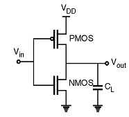
A CMOS Inverter consist of a PMOS & a NMOS. NMOS is considered as a good pull down device whereas PMOS is considered as a good pull up device. So combining PMOS & NMOS in series leads to the formation of CMOS inverter.

The above figure demonstrates the circuit of CMOS Inverter. Now how to size PMOS & NMOS while designing CMOS Inverter that we will discuss while diving in the designing portion later in the editorial. Two different kind of signal can be fed as an Input to CMOS Inverter.
DC Input
When a DC Input is applied to this Circuit. Let’s try to understand how it will behave:
- DC Input =0
If the value of the applied DC input is 0, so the overdrive voltage across NMOS is 0 because Gate terminal will observe 0 whereas the source terminal of NMOS would be at ground/Zero. Talking about PMOS, its Gate terminal is at 0 but the source terminal sees the max potential which is equal to supply. So overdrive seen across PMOS is equal to supply which turn one the PMOS device and output is pulled at supply.
So for Input=0, Output=Supply.
- Dc Input=1 (Supply)
Now let’s understand how CMOS Inverter will behave when logic high input is applied across CMOS Inverter. The working remains same like what we discussed above. Since input is logic high so now NMOS will see overdrive equal to supply as Gate terminal will observe max voltage & Source will be at ground/zero potential. PMOS will see overdrive equal to zero. Since NMOS is on it will pull down the Output to logic 0.
So, for Input=1 (Supply), Output=0
So, far we discussed about the CMOS inverter working when DC input is applied. Now let’s talk about its working when transient input is applied across it.
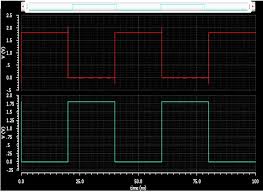
Toggling Input can be considered like this:

If you observe one cycle of this input you can divide its one cycle into 4 segments:
- Input rising from 0 to Supply/logic1
- Constant Logic 1
- Input falling from logic 1 to logic 0/ground
- Constant Logic 0
For constant logic 0 & logic 1 how the CMOS inverter will give its response that we already studied in the above passage. We will be more inclined towards the transient behavior analysis that means when input rising from 0 to logic 1 & when its falling from logic 1 to 0.
Dynamic Characteristic study:
In order to study Dynamic Characteristic of CMOS inverter we will have to analyze from the point when input starts to rise & till the point when input becomes zero after falling.

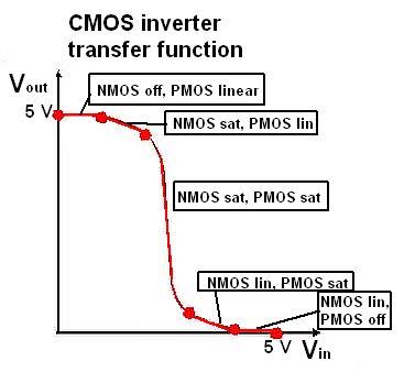
Case 1: When 0<Vin<Vth {NMOS} (Threshold)
In this case, PMOS will be in linear mode whereas NMOS would be turned off.
Case 2: When Vth {NMOS} <Vin<Vdd/2(Supply*0.5)
In this case when input is higher the threshold voltage of MOS but lesser than the half of supply voltage, NMOS will be in saturation mode of operation whereas PMOS will be in linear mode of operation.
Case 3: Vin=0.5*Vdd
When input becomes exactly half of supply voltage in that case NMOS & PMOS both works in saturation mode of operation. In this case CMOS Inverter can work as an amplifier as well.
Case 4: Vdd/2<Vin<Vdd+Vth {PMOS}
When input is higher than the half of supply voltage but lesser than the addition of Supply voltage & PMOS threshold in that case NMOS operates in linear mode whereas PMOS works in Saturation mode.
Case 5: Vdd+Vth {PMOS} <Vin <Vdd
In the last case when input is lesser than the supply voltage but higher than the addition of Supply voltage & PMOS threshold there PMOS is turned off whereas NMOS operates in linear mode of operation.
Power Consumption
CMOS Inverters do not consume any power during static mode of operation whereas they consume power during dynamic operation. Power consumption in dynamic condition depends upon frequency of operation, Supply voltage & load cap which is used for charging & discharging purpose.
In this circuit current flow only happens when input varies from 0 –>1 or 1 –> 0 because at that time NMOS & PMOS respectively discharges & charges the load cap.
Terminologies associated with CMOS Inverter
Trip Point (Vih/Vil): Trip point is that point of input at which Output of CMOS Inverter changes its state. When input is rising up at that time when output changes its state from 1 –> 0 that trip point is known as VIL. VIL is that input voltage below which it is considered as logic 0.
Similarly VIH is that voltage above that any input is considered as logic High. The difference between the VIH & VIL value is known as hysteresis or noise margin of CMOS Inverter circuit. Higher noise margin helps in improving the circuit performance against various noise elements.
Duty Cycle: Duty cycle is basically defined as the ratio of On time of one cycle with respect to the time period. Usually as a designer practice is to design inverter circuit which can generate output with 50% duty cycle considering applied input is also having 50% duty cycle.
Rise Time: Rise time is known as that time which circuit takes to reach from 10% of supply value to 90% of supply voltage when output is rising up.
Fall Time: Fall time is known as the time taken by the circuit to reach from 90% of supply voltage to 10% of supply voltage when output is falling down.
Rise & Fall delay: Rise delay is the delay between rising edge of input to falling edge of CMOS Inverter circuit output at the time when both have reached 50% of its max value. Similarly Fall delay is the delay between the falling edge of input to rising edge of CMOS Inverter output again at the time when input & output both have reached 50% of their max voltages respectively.
Designing of a CMOS Inverter
So, far we have studied about the CMOS Inverter theory and how it behaves against the DC input & Dynamic input. We also studied about the normal structure of it where a PMOS is at the top and stacked with a NMOS. Now we will dive in into the details of its designing.
Beta Factor: This factor is very important in order to design inverter circuit. Beta Factor is basically the ratio of PMOS size to NMOS size in order to keep the same amount of current flow in the circuit. We all know that due to the mobility factor & Threshold difference between NMOS & PMOS current carrying capability of both devices at same width & length ratio differs. In general PMOS offers lower current compare to NMOS at same aspect ratio.
So we need to increase the size of PMOS till that point where its current becomes equal to NMOS. That size ratio between PMOS & NMOS is known as beta factor. In larger tech nodes like 40nm, 22nm, 28nm beta factor value usually comes around 2. But as we move towards lower tech node the value of beta factor is becoming close to 1.
Anyways so the first step in designing of CMOS Inverter is to determine the value of beta factor and scale up the size of PMOS with beta factor scale. Now this CMOS inverter where PMOS size is Beta factor *NMOS aspect ratio can work perfectly at DC input but will it work when dynamic input is applied at higher frequency or not that’s the question?
For that we can use the equation
Power Consumption= Load Cap*(Supply Voltage)^2*Frequency
Through this we can calculate value of Power consumption & then we can use the formula:
Power consumption= Supply Voltage * Current
From here we can calculate the value of current and then from through MOS Current equation we can find out the value of required W/L to support specific frequency & load cap demand.
The other way is to check the duty cycle of CMOS Inverter output at accordingly tune the size of PMOS or NMOS and try to keep the duty cycle of output near to 50. That is more like hit & trial method whereas the above method which we learned that is more calculated way of designing it.
In case if you want to practice the design activity on any tool but you don’t have the license tools available. So, in that case you can use open source CAD tools. At Mosgyan, we have written an article about open source VLSI CAD tools. Here’s the link:
Also as the technology nodes are shrinking the leakage current of device is increasing and the device tolerance limit is scaling down so challenges associated with designs are increasing more & more.
Application of CMOS Inverter in various circuit designs
CMOS Inverter finds its application in various circuits like memories, image sensors & transceivers. In many mobile phones, cameras, servers, modems CMOS Inverter is used.
This circuit is also used in different logic gates & processors. These are also used in level shifting operation from one voltage to other voltage translation. Frequency divider circuit uses CMOS Inverter circuitry. Even in PMIC (Power Management Integrated Circuit) this circuit finds its application.

